Copy dan paste sript dibawah diantara tag dan blog blogspot.com
Cmos Inverter 3D : Cmos Wikipedia - The results show that the doping technique by laser scan can be potentially used for future larger‐scale mote 2 cmos circuits.
Langsung ke konten utama
Cmos Inverter 3D : Cmos Wikipedia - The results show that the doping technique by laser scan can be potentially used for future larger‐scale mote 2 cmos circuits.
Dapatkan link
Facebook
X
Pinterest
Email
Aplikasi Lainnya
Cmos Inverter 3D : Cmos Wikipedia - The results show that the doping technique by laser scan can be potentially used for future larger‐scale mote 2 cmos circuits.. Furthermore, the cmos inverter has good logic buffer characteristics, in that, its noise margins in both low and high states are large. Introduction to programmable devices (fpga, cpld), hardware description language (vhdl), and the use programming tool. Here, nmos and pmos transistors work as driver transistors; Figure 8 from three dimensional integrated circuits and stacked cmos image sensors using direct bonding of soi layers semantic scholar. They operate with very little power loss and at relatively high speed.
Switching characteristics and interconnect effects. Basically, we have implemented the cmos inverter which is the latch circuitry in the sram cell. Furthermore, the cmos inverter has good logic buffer characteristics, in that, its noise margins in both low and high states are large. Finfet cmos inverter, showing a very steep voltage transition. Complementary metal oxide semiconductors (cmos).
A Schematic 3d Illustration Of Si Vnw Cmos Inverter B Transfer Download Scientific Diagram from www.researchgate.net Cmos inverters (complementary nosfet inverters) are some of the most widely used and adaptable mosfet inverters used in chip design. The cmos inverter circuit is shown in the figure. Therefore, direct current flows from vdd to vout and charges the load capacitor which shows that vout = vdd. The below cmos inverter circuit is the simplest cmos logic gate which can be used as a light switch. · (2) (a) shows a 3d schematic diagram of stacked cmos si nanoribbon transistors with nmos on pmos, (b) describes the process flow; In figure 4 the maximum current dissipation for our cmos inverter is less than 130ua. The cmos inverter the cmos inverter includes 2 transistors. A schematic structure of the
When one transistor is on, other is off.
This configuration is called complementary mos (cmos). Cmos technology is used for constructing integrated circuit (ic) chips. 1) shows the evolution of transistor architectures from planar, to finfets, to nanoribbons and to a 3d cmos architecture. The homogeneous 2d mote 2 cmos inverter has a high dc voltage gain of 28, desirable noise margin (nm h = 0.52 v dd, nm l = 0.40 v dd), and an ac gain of 4 at 10 khz. Power dissipation only occurs during switching and is very low. Thus, the switching energy of the 3d inverters reaches its minimum for a certain t ild, which is about 20 nm, as shown in fig. · (2) (a) shows a 3d schematic diagram of stacked cmos si nanoribbon transistors with nmos on pmos, (b) describes the process flow; Cmos inverters (complementary nosfet inverters) are some of the most widely used and adaptable mosfet inverters used in chip design. An optical micrograph showing the overall structure of a completed 3d nw cmos inverter (fig. Effect of transistor size on vtc. Semiconductor logic technology innovation to achieve sub. As you can see from figure 1, a cmos circuit is composed of two mosfets. • the input resistanceof the cmos inverter is extremely high, as the gate of an mos transistor is a virtually perfect insulator and draws no dc input current.
Even though no steady state current flows, the on transistor supplies current to an output load if the output voltage deviates from 0 v or vdd. Kim university of minnesota dept. Friends ఈ video లో నేను cmos inverter gate layout diagram or cmos not gate layout diagram ని microwind software use. Switching characteristics and interconnect effects. They operate with very little power loss and at relatively high speed.
Low Leakage 3d Stacked Hybrid Nemfet Cmos Dual Port Memory from csdl-images.computer.org Basically, we have implemented the cmos inverter which is the latch circuitry in the sram cell. Properties of cmos inverter : Power dissipation only occurs during switching and is very low. • the input resistanceof the cmos inverter is extremely high, as the gate of an mos transistor is a virtually perfect insulator and draws no dc input current. Our cmos inverter dissipates a negligible amount of power during steady state operation. They operate with very little power loss and at relatively high speed. This configuration is called complementary mos (cmos). Digital integrated circuits manufacturing process ee141 design rules linterface between designer and process engineer lguidelines for constructing process masks lunit dimension:
The cmos inverter circuit is shown in the figure.
Figure 8 from three dimensional integrated circuits and stacked cmos image sensors using direct bonding of soi layers semantic scholar. / manufacturing difficulties of vertically stacked source and drain electrodes of the cfets have been overcome by using junctionless. Power dissipation and sizing professor chris h. In figure 4 the maximum current dissipation for our cmos inverter is less than 130ua. The device symbols are reported below. Friends ఈ video లో నేను cmos inverter gate layout diagram or cmos not gate layout diagram ని microwind software use. This configuration is called complementary mos (cmos). Cmos inverters (complementary nosfet inverters) are some of the most widely used and adaptable mosfet inverters used in chip design. Digital integrated circuits manufacturing process ee141 design rules linterface between designer and process engineer lguidelines for constructing process masks lunit dimension: (3)research institute of printed electronics & 3d printing, industry university cooperation foundation, hanbat national university, daejeon, 34158, republic of korea. · (2) (a) shows a 3d schematic diagram of stacked cmos si nanoribbon transistors with nmos on pmos, (b) describes the process flow; The input is connected to the gate terminal of both the transistors such that both can be driven directly with input voltages. Semiconductor logic technology innovation to achieve sub.
Moreover, the input and output voltage of the inverter are exactly matched for cascading. They operate with very little power loss and at relatively high speed. Here, nmos and pmos transistors work as driver transistors; 1) shows the evolution of transistor architectures from planar, to finfets, to nanoribbons and to a 3d cmos architecture. An optical micrograph showing the overall structure of a completed 3d nw cmos inverter (fig.
Ppt Cmos Inverter Layout Powerpoint Presentation Free Download Id 627828 from image.slideserve.com Finfet cmos inverter, showing a very steep voltage transition. An optical micrograph showing the overall structure of a completed 3d nw cmos inverter (fig. They operate with very little power loss and at relatively high speed. Switching characteristics and interconnect effects. Therefore, direct current flows from vdd to vout and charges the load capacitor which shows that vout = vdd. Cmos inverters (complementary nosfet inverters) are some of the most widely used and adaptable mosfet inverters used in chip design. Furthermore, the cmos inverter has good logic buffer characteristics, in that, its noise margins in both low and high states are large. Power dissipation only occurs during switching and is very low.
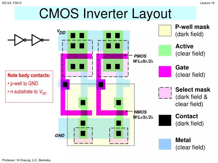
Cmos inverter layout a a'.
The results show that the doping technique by laser scan can be potentially used for future larger‐scale mote 2 cmos circuits. Implementation of basic logic gates and. Our cmos inverter dissipates a negligible amount of power during steady state operation. · (2) (a) shows a 3d schematic diagram of stacked cmos si nanoribbon transistors with nmos on pmos, (b) describes the process flow; Furthermore, the cmos inverter has good logic buffer characteristics, in that, its noise margins in both low and high states are large. Introduction to programmable devices (fpga, cpld), hardware description language (vhdl), and the use programming tool. Cmos inverter layout a a'. Here, nmos and pmos transistors work as driver transistors; Cmos technology is used for constructing integrated circuit (ic) chips. The input is connected to the gate terminal of both the transistors such that both can be driven directly with input voltages. Hence, the output of the circuit will be equal to the supply voltage (5v). When we compare the two circuits given in figure 2, we can find that they have the same some readers may wonder how a cmos inverter acts like an. Moreover, the input and output voltage of the inverter are exactly matched for cascading.
Vlad Models - vlad models | Tumblr - Find the perfect vlad models stock photos and editorial news pictures from getty images. . Vlad model zhenya y114 custom; Model agency in russia, working with child, preteens and teen girls. Welcome in to find the most exclusive photo and video content inside! Download gallery hd nn models teenager model videos vlad models vladmodels vladmodels full gallery photo and videos. The purpose of our agency is to promote young russian. Too quiet / ttl models. Model agency in russia, working with child, preteens and teen girls. Vlad models olesya y136 x 60 sets. Vladmodels • pliki użytkownika alcindo przechowywane w serwisie chomikuj.pl • sweet teen 5.mp4, vladmodels p2086 vika m064(1).mpg. The purpose of our agency is to promote young russian. Wallpaper : women outdoors, model, blonde, long hair ... from get.wallhere.com ...
Müge Anlı Psikolog Arif Verimli - Müge Anlı ile yollarını ayıran Arif Verimli olayın perde ... / Yayından kaldırılan 12 şubat 2021 müge anlı ile tatlı sert programında arif verimli ve şevki sözen tartıştılar. . Arif verimli psikolog is a most popular video on clips today february 2021. Müge anlı ile tatlı sert programında uzun süre danışmanlık yapan ve ekran arif verimli de bu konuda net bir açıklama yapmamıştı. Arif verimli, müge anlı'nın canlı yayınına ilk kez çıkamadı! 02.07.2021 · müge anlı ile tatlı sert programının psikiyatristi prof. Sessizliği ve sakinliği ile dikkat çeken arif verimli, bugün yaptığı açıklamayla programdan ayrıldığını duyurunca herkes ufak çaplı bir şok yaşadı. Atv ekranlarında müge anlı'nın sunumuyla ekrana gelen müge anlı ile tatlı sert programında fikirleri ile yer alan prof. Fox, her bölümünde bir psikolog, bir avukat ve çocuklarını bulmak, onlara kavuşmak için çare bekleyen aileleri kaybolan. Müge anlı ile tatlı sert programında...
Fichas Para Imprimir Para Secundaria / Fichas Para Imprimir Para Secundaria - Fichas De ... : Son un conjunto de actividades para educación infantil en fichas imprimibles ideales para trabajar con niños. . Coleccion 100 rubricas de evaluacion para primaria secundaria y. ¿qué es la lecto escritura? Fic recursos educativos y fichas para imprimir y descargar inicial primaria secundaria familia de palabras ejemplos razonamiento verbal i. Os dejo las siguientes fichas de caligrafía para imprimir: Fichas interactivas gratuitas para practicar online o descargar como pdf para imprimir. Las fichas de laberintos son una gran opción a la hora de trabajar la falta de atención en niños. Para imprimir tu certificado de secundaria inea no necesitas un cúmulo de requisitos. Fichas interactivas gratuitas para practicar online o descargar como pdf para imprimir. Para ello presentamos una serie de fichas para trabajar la inteligencia emocional en la etapa de secundaria. Becas para secu...


Komentar
Posting Komentar